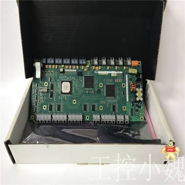
¥ 价格面议
¥ 价格面议
¥ 价格面议
¥ 价格面议
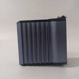
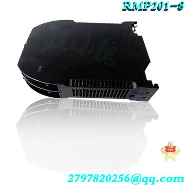
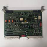
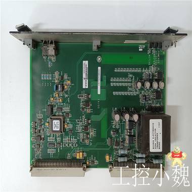
易卖工控网(www.ymgk.com)提供”KONGSBERG控制器模块HIPAP APC12 331890”,产品详情:品牌/厂家:KONGSBERG、型号:HIPAP APC12 331890、成色:全新、货期:现货 1天内发货、保修:180天,更多产品详情就上易卖工控网。
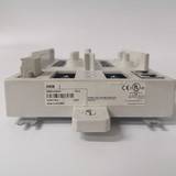
Multilin制造的电机管理继电器。控制电源为50- 300 VDC/40-265 VAC。此继电器上没有可选RTD输入。该装置包括一个可选的计量包。没有可选的光纤端口。该继电器为三相电机及其相关系统提供保护和监控。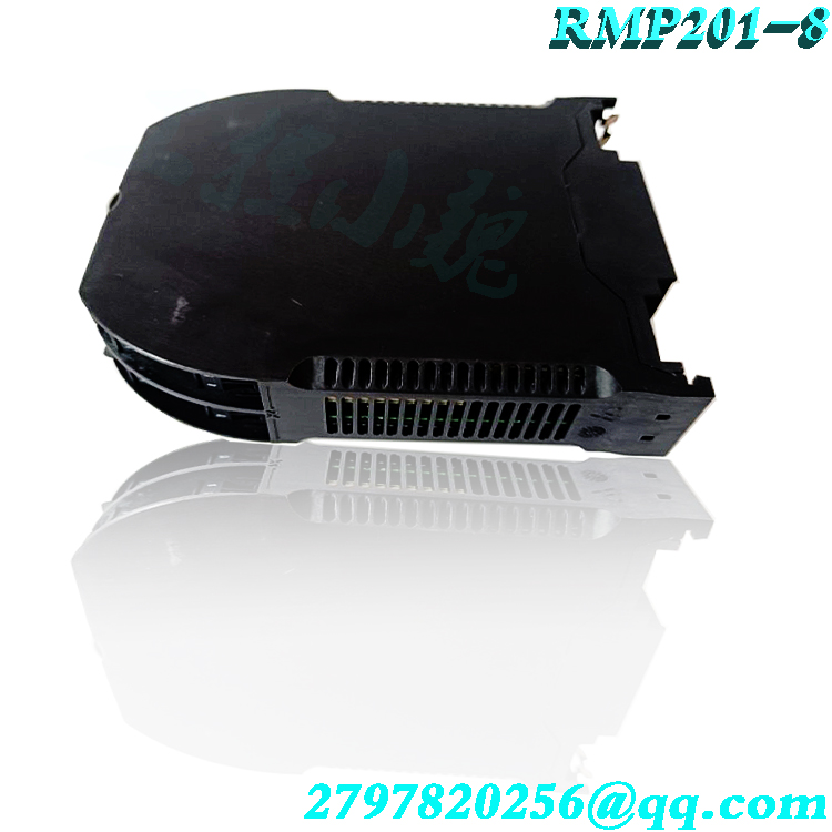 369可以“学习”各个电机参数,并适应各个应用。为了提高继电器的保护能力,用户可以调整电机浪涌电流、冷却速度和/或加速时间。如果您对该电机管理继电器或相关系列或制造商有任何疑问,请联系AX Control。 设定点键允许用户浏览可编程参数页面标题。实际值键允许用户浏览测量参数页面标题。页面向上和向下键可用于滚动页面标题,查看实际值和设定点。
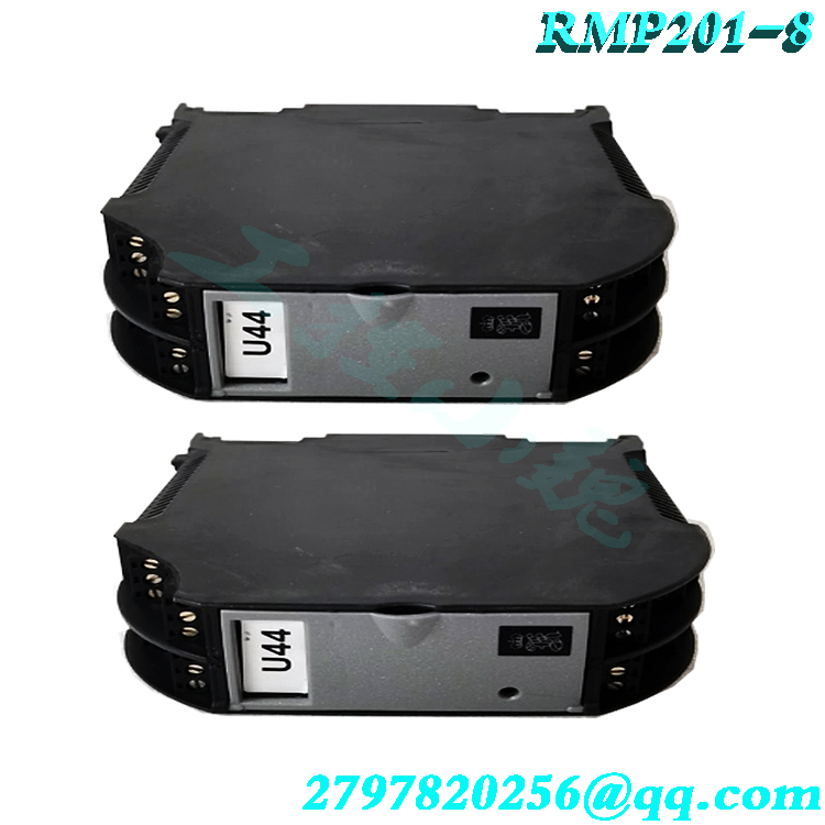 上下对齐键可用于滚动浏览副标题。值向上和向下键允许用户滚动浏览设定点编程模式中的变量。重置键允许用户重置跳闸或锁定报警。输入键可以输入子组或存储更改的设定值。清除键可以退出子组或将更改的设定点返回到其原始值。对于上下文相关的帮助消息,可以随时按帮助键。 应始终确保369-HI- 0-M-0-0-E正确接地。必须将安全接地和过滤器接地(分别为端子126和123)连接到主接地母线,以正确接地装置。 关于369-HI-0-M-0-0-E的常见问题 369-LO-0-M-F-E-0-E电机管理继电器的控制电源规格是什么? 369-LO-0-M-F-E-0-E具有低 (LO)控制功率规格。
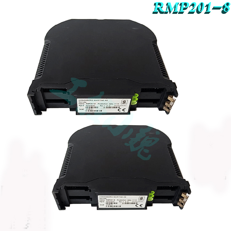 VDC范围为20-60,此369 Multilin电机管理继电器的VAC控制功率范围为20 至48。此低规格与高(HI)选项相比,后者为50-300 VDC和60-265 VAC控制电源。 369-LO-0-M-F- E-0-E Multilin General Electric数字继电器有哪些附加功能? 369-LO-0-M-F-E-0-E的其他功能是可选的计量包。除了基本单元的单个模拟输出外,该软件包还提供三个额外的可配置模拟输出。该软件包还为装置提供了功率和电压元件的输入,能够测量各种具体参数,如V、kW等。 369- LO-0-M-F-E-0-E还包含由(F)选项表示的可选光纤端口。此光纤数据链路用于更恶劣的环境或RRTD连接。光纤尺寸为50/125、62.5/125、100/140和200 微米。LED发射器类型为820 nm LED,具有多模特性。 369-LO-0-M-F-E-0-E的可选光纤端口的用途是什么? 369-LO-0-M-F-E-0-E的光纤端口( 选项F)的用途是允许远程模块RTD连接到电机管理继电器。The most popular and commonly used power electronic switch devices are the Bipolar Junction Transistor BJT and the MOSFET. We have already discussed in detail about the working of BJT and the working of MOSFET and how they are used in circuits. But, both these components had some limitations to be used in very high current applications. So, we moved another popular power electronic switching device called the IGBT. You can think of IGBT as a fusion between BJT and MOSFET, these components have the input characteristics of a BJT and output characteristics of a MOSFET. In this article, we get familiar with the basics of IGBT, how they work, and how to use them in your circuit designs. IGBT is the short form of Insulated Gate Bipolar Transistor. It is a three-terminal semiconductor switching device that can be used for fast switching with high efficiency in many types of electronic devices. These devices are mostly used in amplifiers for switching/processing complex wave patters with pulse width modulation (PWM). The typical symbol of IGBT along with its image is shown below.As mentioned earlier an IGBT is a fusion between a BJT and MOSFET. The symbol of the IGBT also represents the same, as you can see the input side represents a MOSFET with a Gate terminal and the output side represents a BJT with Collector and Emitter. The Collector and the Emitter are the conduction terminals and the gate is the control terminal with which the switching operation is controlled. IGBT can be constructed with the equivalent circuit that consists of two transistors and MOSFET, as the IGBT posses the output of the below combination of the PNP transistor, NPN transistor, and MOSFET. IGBT combines the low saturation voltage of a transistor with the high input impedance and switching speed of a MOSFET. The outcome obtained from this combination delivers the output switching and conduction characteristics of a bipolar transistor, but the voltage is controlled like a MOSFET.Since IGBT is the combination of MOSFET and BJT they are also called by different names. The different names of IGBT are Insulated Gate Transistor( IGT), Metal Oxide Insulated Gate Transistor (MOSIGT), Gain Modulated Field Effect Transistor (GEMFET), Conductively Modulated Field Effect Transistor (COMFET).IGBT has three terminals attached to three different metal layers, the metal layer of the gate terminal is insulated from the semiconductors by a layer of silicon dioxide (SIO2). IGBT is constructed with 4 layers of semiconductor sandwiched together. The layer closer to the collector is the p+ substrate layer above that is the n- layer, another p layer is kept closer to the emitter and inside the p layer, we have the n+ layers. The junction between the p+ layer and n- layer is called the junction J2 and the junction between the n- layer and the p layer is called the junction J1. The structure of IGBT is shown in the figure understand the working of the IGBT, consider a voltage source VG connected positively to the Gate terminal with respect to the Emitter. Consider other voltage source VCC connected across The Emitter and the Collector, where Collector is kept positive with respect to the Emitter. Due to the voltage source VCC the junction J1 will be forward-biased whereas the junction J2 will be reverse biased.

 记住账号
记住账号


 收藏商品
收藏商品


 2778087246
 18150367963