
¥ 价格面议

¥ 价格面议
¥ 价格面议

¥ 价格面议
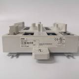
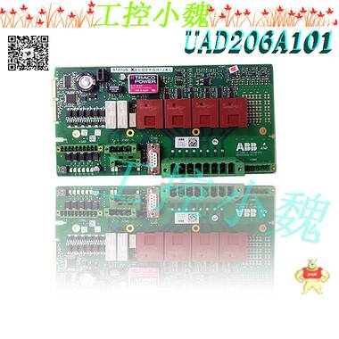
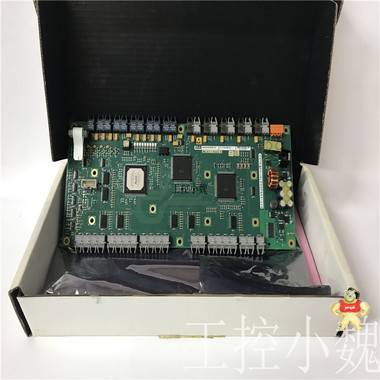
易卖工控网(www.ymgk.com)提供”3BHE019959P201AEND:C模块ABB”,产品详情:品牌/厂家:ABB、型号:3BHE019959P201AENDC、成色:全新、货期:现货 1天内发货、保修:180天,更多产品详情就上易卖工控网。
3BHE019959P201AEND:C转子弯曲:为什么转子弯曲经常作为偏差处理,旋转的弯曲产生1X信号?机械故障诊断中,动态振动信号的1X成分是有用的。当研究机械的同步响应时,弯曲产生的信号要进行补偿,位移传感器噪声源转子弯曲–如果转子弯曲是0久性的,就可以按1X噪声源处理–某些弯曲,是不稳定的,会随着温度和负荷变化,这类弯曲如果具有可重复性,也可以按照噪声处理。轴裂纹产生的弯曲随裂纹的扩展而变化,且不具有重复性。三个定时器都使用一个中断IRQ5。定时器中断状态寄存器用于确定哪些计时器启动了中断。中断状态寄存器是一个通用输入寄存器,位于82C54外部,位于从电源管理基输入/输出地址偏移31h。中断状态寄存器地址可以通过首先确定PCI配置基址来找到对于设备ID 7113h和供应商ID 8086h。电源管理基本输入/输出地址可以通过从此PCI配置地址读取偏移量40h来找到。
 计时器中断状态寄存器位位于电源管理的偏移量31h处基址输入/输出地址,位5、6和7(参见图4-2)。从电源管理基本输入/输出地址读取偏移量31h的字节用于获取这些位。位5、6和7分别对应于计时器2、1和0,为了计时器中断状态寄存器,首先将零(0)写入通用输出寄存器,位于电源管理基座的偏移37h输入/输出地址位3、4和6(不是位3、4和5)。然后将1写在相同的重新启用定时器中断状态寄存器的位。位3、4和6对应于定时器2、1和0分别使用PC/AT的标准程序定时器中断IRQ5。有关使用82C54定时器的示例,请参阅附录D。VMIVME-7698计时器从500美元开始映射到输入/输出地址空间。请参阅表4-1计时器,由三个16位计时器和一个控制字寄存器组成(见图4-4)通过8位数据总线读取/写入。定时器0、1和2这三个定时器在功能上是等效的。因此,只有
将描述单个计时器。图4-5是计时器的框图。每个计时器功能独立。尽管控制字显示在计时器块中它不是计时器的一部分,但其内容直接影响计时器的工作方式功能。如图4-5所示,当锁存时,状态寄存器包含当前控制字寄存器的内容以及输出和负载的当前状态计数标志(状态字可通过Read Back命令获得,请参阅第59页的“阅读”部分)。计时器标记为TE(计时器元素)。它是一个16位同步可预设向下柜台标记为OLM和OLL的块是8位输出锁存器(OL)。下标M和L代表0高有效字节和0低有效字节。这些插销通常跟踪TE,但在收到命令时,将锁定并保持当前计数,直到CPU读取计数。读取锁存计数时,OL寄存器将继续跟踪TE。读取OL寄存器时,必须执行两次8位访问以检索计时器的完整16位值,因为一次只启用一个锁存器。TE无法读取;从OL寄存器读取计数。A single interrupt, IRQ5, is used by all three Timers. A Timer Interrupt Status register
is provided in order to determine which Timer(s) initiated an interrupt. The interrupt
status register is a general-purpose input register located, external to the 82C54, at
offset 31h from the Power Management base I/O address. The interrupt status
register address can be found by first determining the PCI Configuration base address
for Device ID 7113h and Vendor ID 8086h. The Power Management base I/O address
can be found by reading offset 40h from this PCI Configuration address. The Timer
Interrupt Status register bits are located at offset 31h from the Power Management
base I/O address, bits 5, 6, and 7 (refer to Figure 4-2).A byte read of Offset 31h from the Power Management base I/O address is used to
obtain these bits. Bits 5, 6, and 7 correspond to Timers 2, 1, and 0, respectivelyIn order to clear the Timer Interrupt Status register, first write zeros (0’s) to the
general-purpose output register located at offset 37h of the Power Management base
I/O address bits 3, 4, and 6 (Not bits 3, 4 and 5). Then write ones (1’s) to these same
bits to re-enable the Timer Interrupt Status register. Bits 3, 4, and 6 correspond to
Timers 2, 1, and 0, respectivelyThe Timer Interrupts are cleared using the standard procedure for clearing PC/AT
IRQ5. Refer to Appendix D for an example of using the 82C54 timers.The VMIVME-7698 Timers are mapped in I/O address space starting at $500. See
Table 4-1. The Timers, consisting of three 16-bit timers and a Control Word Register
(see Figure 4-4) are read from/written to via an 8-bit data bus.The three Timers, Timer 0, 1, and 2, are functionally equivalent. Therefore only a
single Timer will be described. Figure 4-5 is a block diagram of a Timer. Each Timer is
functionally independent. Although the Control word is shown in the Timer block
diagram, it is not a part of the Timer, but its contents directly affect how the Timer现场运维工单派遣频繁,24小时ON CALL没商量?ABB助力运维法方式升级,从周期性运维到状态运维和预测性运维,预判你的预判,助你成为运筹帷幄的“全知全能”。
ABB从多年环网柜设计、制造和运行经验出发,开发出众多具有针对性的智能监测和诊断算法,用以实现设备由周期性运维到状态运维和预测性运维的转变,从而减少现场运维工单的派遣,节约人力。ABB基于真实设备数据的算法开发,大幅提高了监测诊断的准确率,更率先提出了自学习动态阈值的理念,直面设备个体差异,实现阈值的实时调整、自动调整,精准识别判断设备运行状态,让设备运维更省心夏日是度假休憩的季节,如何能顶着炎炎烈日、在设备前稳坐如钟?ABB多样化用户交互手段让你不再苦守现场一卷到底,远程亦可便捷进行信息交互,不被工作束缚远行的步伐,轻松享受盛夏。
ABB数字智能环网柜Safe Digital可以自由接入ABB Ability™ 云端平台,实现数据的远程访问,多种数据查看途径让你随时随地掌控设备情况:可通过柜体上的显示屏,查看所有设备运行数据和设备健康状态;可通过扫描0码,使用手机连接智能终端WiFi,通过手机浏览设备监测实时数据;可搭乘“云边融合”的快车,通过ABB Ability™云端平台(或客户私有平台)查看数据情况。重要事件信息及时推送到客户订阅手机号,实现设备状态“零延时”掌握。ABB数字智能环网柜Safe Digital不仅性能优越,还在设计中考虑了易更换性,便于二次设备升级改造。通过更简单的计划和更少的改造投入实现设备全寿命周期的成本降低,全面呵护客户的资产健康,提高客户资产的投资价值。
具有出色 TFT/LED 显示颜色和多协议连接性的触摸屏面板。它们是易于使用的 HMI,具有全面和集成的模板和库,适用于您需要的每个可能的过程。
所有标准面板均配备 TFT/LED 显示屏中的高分辨率图形。大多数型号提供宽屏、高分辨率显示屏,以提高效率和出色的操作员交互。
完全可部署的 HMI,具有适用于每个可以想象的过程的全面和集成的模板和库。Panel Builder 工具具有熟悉的 Microsoft® Windows® 环境以及多语言支持,可实现快速、简单和高效的工程设计。81001-450-53-R当写入该字段时,定时器4在下一次上升时加载写入的值计时器时钟的边缘,无论计时器是启用还是禁用。这个存储在该寄存器中的值也会在终端计数时自动重新加载(或超时)。读取任一字段时,当前计数值被锁定并返回。有两种模式确定如何锁定计数,具体取决于WDT控制状态寄存器(CSR2)中的“读取锁存选择”位。参见CSR2有关这两种模式的更多信息,请注册说明。读取此字段时,当前计数值被锁定并返回。有两种模式确定如何锁定计数,具体取决于WDT控制状态寄存器(CSR2)中的“读取锁存选择”位。参见CSR2有关这两种模式的更多信息,请注册说明。定时器4电流计数寄存器(TMRCCR4)定时器4的电流计数可通过定时器4电流计数寄存器读取(TMRCCR4),位于BAR2中地址的偏移量0x28处81001-450-53-R A-B高压变频器模块
I.中央处理单元(CPU)
中央处理单元(CPU)是PLC的控制中枢。它按照PLC系统程序赋予的功能接收并
存储从编程器输入的用户程序和数据,检查电源、存储器、VO以及警戒定时器的状态,
并能诊断用户程序中的语法错误:当PLC投入运行时,首先它以扫描的方式接收现场各输
入装置的状态和数据,并分别存入IO映像区,然后从用户程序存储器中逐条读取用户程
序,经过命令解释后,按指令的规定将逻辑或算术运算的结果送入Vo映像区或数据寄存
器内。等所有的用户程序执行完毕之后,0后将1/O映像区的各输出状态或输出寄存器内
的数据传送到相应的输出装置,如此循环运行,直到停止运行为止。
为了进一步提高PLC的可靠性,近年来对大型PLC还采用双CPU构成冗余系统,或
采用三CPU的表决式系统。这样,即使某个CPU出现故障,整个系统仍能正常运行。
2.存储器
存放系统软件的存储器称为系统程序存储器。
(1) PLC常用的存储器类型。
1) RAM (Random Assess Memory)。这是-一种读/写存储器(随机存储器)其存取速
度0快,由铿电池支持。
2) EPROM (Erasable Progranmable Read Only Memory)。这是一种可擦除的只读存储
器在断电情况下存储器内的所有内容保持不变(在紫外线连续照射下可擦除存储器内容)。
3) EPROM (Electrical Erasable Programmable Read Only Memory)。这是一种电可擦
除的只读存储器。使用编程器就能很容易地对其所存储的内容进行修改。
(2) PLC存储空间的分配。虽然各种PLC的CPU的0大寻址空间各不相同,但是根
据PLC的工作原理其存储空间一般包括以下三个区域:系统程序存储区、系统RAM存储
区(包括I/O映像区和系统软设备等)、用户程序存储区。
1)系统程序存储区。在系统程序存储区中存放着相当于计算机操作系统的系统程序,
包括监控程序、管理程序、命令解释程序、功能子程序、系统诊断子程序等。由制造厂商
将其固化在EPROM中,用户不能直接存取。它和硬件一起决定了 该PLC的性能。
2)系统RAM存储区。系统RAM存储区包括I/O映像区以及各类软设备,如:逻辑
线圈、数据寄存器、计时器、计数器、变址寄存器、累加器等存储器。组态控制技术属于一种计算机控制技术。它是利用计算机监控某种设备使其按照控制要求工作。利用组态控制技术构成的计算机组态监控系统主要由被控对象、传感器、I/O接口、计算机及执行机构等部分组成。
本次实训是借助MCGS组态软件平台来完成组态监控系统人机界面制作和程序的设计的。MCGS(Monitor and Control Generated System, 通用监控系统)组态软件是北京昆仑通态软件公司研发的基于Window平台的,用于快速构造和生成上位机监控系统的组态软件系统。通过对现场数据的采集处理,以动画显示、报警处理、流程控制、报表输出等和多种方式向用户提供解决实际工程问题的开发平台。
由于是国人开发的软件,所以它是全中文的,很适合我们使用,还有它可提供近百种绘图工具和基本图符,快速构造图形界面,此外还提供上千个精美的图库元件及渐进色等多种
动画方式可以快速的构建精美的动画,它还支持温控曲、计划曲线、时实曲线、历史曲线、XY等多种工控曲线。总之使用MCGS软件可以较快速的完成一个运行稳定、功能成熟、维护量小并且具备专业水准的计算机监控控制系统的开发工作。下面我来介绍在使用MCGS组态软件来完成任务的详细过程及遇到的问题和解决的办法。
任务一 水泵运行控制
打开MCGS通用版组态软件,我们会看见5个部分,分别为主控窗口、设备窗口、用户窗口、实时数据库和运行策略。
首先我们先新建一个工程,将其命名为水泵控制系统并进行保存。
然后打开用户窗口完成相关图符的建立,老师在建工程时先建立了实时数据库,是因为对图符的控制属性有较清楚的认识,所以对于初学者来说,先画图符是0先的选择。
(1)在用户窗口中新建一个窗口0,并将其重命名水泵运行控制,在动画窗口中用标签建立动画的标题“水泵控制”
(2)绘制水泵
在软件中,已经为我们提供了“对象原件库”我们可以在其中选择所要的原件,所以接下来添加一个“泵30”图符再确定,可以调节图符的大小,以至达到美观的效果
(3)在泵下面添加两个“按钮”分别将名称改为“启动”和“停止”也可以双击来改变按钮的背景颜色。
(4)因为要展示停止和启动时的状态所以再添加两个指示灯,为了更为清楚的展现启动和停止的状态,也可以自己改造一个指示灯,其改造方法为先用一个库提供的指示灯作为改造对象先分解单元在将0前面的图符拖走,将底层的图符分解图符再改变其颜色和添加一个“可见度”属性并在表达式里填入@开关量,然后再对另一只指示灯做相关属性的设置。
(5)为了显示时间我们再添加两个按钮分别为“定时器启动”和“定时器复位”再添加 两个标签分别为控制“计时时间”和“时间到”。
Rotor bending: why is the rotor bending often treated as deviation, and the rotating bending generates 1x signal? The 1x component of dynamic vibration signal is useful in mechanical fault diagnosis. When studying the synchronous response of the machine,
Noise source of displacement sensor
Rotor bending – if rotor bending is permanent, it can be treated as 1x noise source – some bending is unstable and will change with temperature and load. If such bending is repeatable, it can also be treated as noise. The bending caused by the axial crack varies with the crack propagation and has no repeatability. All three timers use an interrupt irq5. The timer interrupt status register is used to determine which timers initiated interrupts. The interrupt status register is a general-purpose input register, which is located outside the 82C54 and offset 31h from the input / output address of the power management base. The interrupt status register address can be found for the device ID 7113h and the vendor ID 8086h by first determining the PCI configuration base address. The power management basic input / output address can be found by reading the offset 40H from this PCI configuration address. The timer interrupt status register bit is located at the base address input / output address at the offset 31h of the power management, bits 5, 6 and 7 (see Fig. 4-2). The byte of offset 31h is read from the power management basic input / output address for acquiring these bits. Bits 5, 6 and 7 correspond to timers 2, 1 and 0 respectively. For the timer interrupt status register, zero (0) is first written to the general output register, which is located at offset 37h input / output address bits 3, 4 and 6 (not bits 3, 4 and 5) of the power management base. Then write 1 to the same bit of the re enable timer interrupt status register. Bits 3, 4 and 6 correspond to timers 2, 1 and 0 respectively interrupt irq5 using the standard program timer of PC / at. See Appendix D for an example of using the 82C54 timer. The vmivme-7698 timer maps to the input / output address space from $500. Refer to table 4-1. The timer is composed of three 16 bit timers and a control word register (see Figure 4-4) and is read / written through the 8-bit data bus. Timers 0, 1 and 2 are functionally equivalent. Therefore, only
A single timer will be described. Fig. 4-5 is a block diagram of a timer. Each timer functions independently. Although the control word is displayed in the timer block, it is not a part of the timer, but its content directly affects the working mode and function of the timer. As shown in Figure 4-5, when latched, the status register contains the contents of the current control word register and the current status count flag of the output and load (the status word can be obtained through the read back command, see the "reading" section on page 59). The timer is marked te (timer element). It is a 16 bit synchronous presettable block marked as OLM and oll and is an 8-bit output latch (OL). Subscripts m and l represent the most significant byte and the least significant byte. These pins usually track te, but when a command is received, they lock and hold the current count until the CPU reads the count. When the latch count is read, the ol register will continue to track te. When reading the ol register, you must perform two 8-bit accesses to retrieve the full 16 bit value of the timer because only one latch is enabled at a time. Te cannot be read; Read the count from the ol register. A single interrupt, IRQ5, is used by all three Timers. A Timer Interrupt Status register
is provided in order to determine which Timer(s) initiated an interrupt. The interrupt
status register is a general-purpose input register located, external to the 82C54, at
offset 31h from the Power Management base I/O address. The interrupt status
register address can be found by first determining the PCI Configuration base address
for Device ID 7113h and Vendor ID 8086h. The Power Management base I/O address
can be found by reading offset 40h from this PCI Configuration address. The Timer
Interrupt Status register bits are located at offset 31h from the Power Management
base I/O address, bits 5, 6, and 7 (refer to Figure 4-2). A byte read of Offset 31h from the Power Management base I/O address is used to
obtain these bits. Bits 5, 6, and 7 correspond to Timers 2, 1, and 0, respectivelyIn order to clear the Timer Interrupt Status register, first write zeros (0’s) to the
general-purpose output register located at offset 37h of the Power Management base
I/O address bits 3, 4, and 6 (Not bits 3, 4 and 5). Then write ones (1’s) to these same
bits to re-enable the Timer Interrupt Status register. Bits 3, 4, and 6 correspond to
Timers 2, 1, and 0, respectivelyThe Timer Interrupts are cleared using the standard procedure for clearing PC/AT
IRQ5. Refer to Appendix D for an example of using the 82C54 timers. The VMIVME-7698 Timers are mapped in I/O address space starting at $500. See
Table 4-1. The Timers, consisting of three 16-bit timers and a Control Word Register
(see Figure 4-4) are read from/written to via an 8-bit data bus. The three Timers, Timer 0, 1, and 2, are functionally equivalent. Therefore only a
single Timer will be described. Figure 4-5 is a block diagram of a Timer. Each Timer is
functionally independent. Although the Control word is shown in the Timer block
Diagram, it is not a part of the timer, but its contents directly affect how the timer on-site operation and maintenance work orders are dispatched frequently, and 24-hour on call is not discussed? ABB helps to upgrade the operation and maintenance method, from periodic operation and maintenance to state operation and maintenance and predictive operation and maintenance, to predict your prediction and help you become a "omniscient and omnipotent" strategist.
Based on years of experience in the design, manufacturing and operation of ring network cabinets, abb has developed many targeted intelligent monitoring and diagnosis algorithms to realize the transformation of equipment from periodic operation and maintenance to state operation and maintenance and predictive operation and maintenance, so as to reduce the dispatch of on-site operation and maintenance orders and save manpower. ABB's algorithm development based on real equipment data has greatly improved the accuracy of monitoring and diagnosis. It also took the lead in putting forward the concept of self-learning dynamic threshold, directly facing the individual differences of equipment, realizing real-time adjustment and automatic adjustment of threshold, accurately identifying and judging the operating status of equipment, and making equipment operation and maintenance more worry free. Summer is a holiday and rest season. How can you stand in front of the equipment in the scorching sun? ABB's diversified user interaction means make you no longer have to wait on the site to the end. Remote information interaction can also be carried out conveniently, and you can easily enjoy the midsummer without being bound by work.
ABB digital intelligent ring main cabinet (safe digital) can freely access ABB ability ™ The cloud platform realizes remote access to data, and multiple data viewing ways allow you to control the equipment at any time and anywhere: you can view all equipment operation data and equipment health status through the display screen on the cabinet; It can scan the QR code, use the mobile phone to connect to the WiFi of the smart terminal, and monitor the real-time data through the mobile phone browsing device; You can take the express train of "cloud edge integration" through ABB ability ™ Cloud platform (or customer private platform) to view data. The important event information is timely pushed to the mobile phone number subscribed by the customer to realize the "zero delay" of the equipment status. ABB digital intelligent ring main cabinet safe digital not only has superior performance, but also takes into account the easy replacement in the design, which is convenient for the upgrading and transformation of secondary equipment. Through simpler planning and less transformation investment, the cost of the whole life cycle of equipment can be reduced, the health of customers' assets can be fully protected, and the investment value of customers' assets can be improved.
Touch screen panel with excellent TFT / LED display color and multi protocol connectivity. They are easy-to-use HMIS with comprehensive and integrated templates and libraries for every possible process you need.
All standard panels are equipped with high-resolution graphics in TFT / LED displays. Most models offer a wide screen, high-resolution display to improve efficiency and excellent operator interaction.
Fully deployable HMI with comprehensive and integrated templates and libraries for every conceivable process. Panel builder tool has familiar Microsoft ® Windows ® Environment and multi language support can realize fast, simple and efficient engineering design. 81001-450-53-r when writing this field, timer 4 loads the edge of the written value timer clock at the next rise, whether the timer is enabled or disabled. The value stored in this register will also be automatically reloaded (or timed out) when the terminal counts. When reading any field, the current count value is locked and returned. There are two modes to determine how to lock the count, depending on the "read latch select" bit in the WDT control status register (csr2). See csr2 for more information on these two modes, see the registration instructions. When reading this field, the current count value is locked and returned. There are two modes to determine how to lock the count, depending on the "read latch select" bit in the WDT control status register (csr2). See csr2 for more information on these two modes, see the registration instructions. Timer 4 current count register (tmrccr4) the current count of timer 4 can be read through the timer 4 current count register (tmrccr4), located at the offset 0x28 of address in bar2 81001-450-53-r A-B high voltage inverter module
1. Central processing unit (CPU)
The central processing unit (CPU) is the control center of PLC. It receives and transmits the data according to the functions given by the PLC system program
Store user programs and data input from the programmer and check the status of power supply, memory, VO and alarm timer,
It can also diagnose syntax errors in the user program: when the PLC is put into operation, it first receives the field inputs in the form of scanning
Enter the status and data of the device, and store them in the IO image area, and then read the user program from the user program memory one by one
After the command is interpreted, the result of logical or arithmetic operation is sent to the VO image area or data register according to the instruction
Inside. After all user programs are executed, the output states or output registers of the 1 / O image area are finally
The data is transmitted to the corresponding output device, and the operation is repeated until the operation is stopped.
In order to further improve the reliability of PLC, in recent years, large-scale PLC has also adopted Dual CPU to form redundant system, or
Voting system with three CPUs. In this way, even if a CPU fails, the whole system can still operate normally.
2. Memory
The memory storing system software is called system program memory.
(1) Memory type commonly used by PLC.
1) RAM (Random Assess Memory)。 This is - a read / write memory (random access memory) whose access speed
The fastest speed, supported by Keng battery.
2) EPROM (Erasable Progranmable Read Only Memory)。 This is an erasable read-only storage
All contents in the memory remain unchanged when the device is powered off (the memory contents can be erased under continuous ultraviolet irradiation).

 记住账号
记住账号


 收藏商品
收藏商品


 2778087246
 18150367963