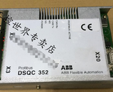
¥ 1495.00
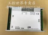
¥ 1495.00
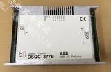
¥ 1495.00
¥ 1495.00
¥ 1495.00
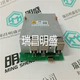
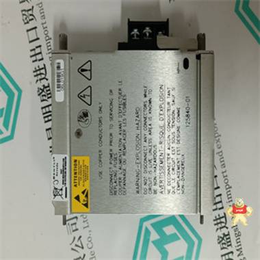
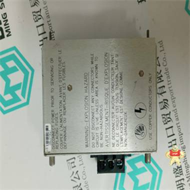
易卖工控网(www.ymgk.com)提供”125840-01模块备件”,产品详情:品牌/厂家:Associated-507967、型号:125840-01、成色:全新、货期:现货 1天内发货、保修:180天,更多产品详情就上易卖工控网。
125840-01
DSC1033是一款3.3V固定频率MEMS
基于纯硅™ 振荡器。它可以是一个工厂
编程设定为1到10之间的任何频率
150MHz。
DSC1033采用了全硅芯片
谐振器,非常坚固,几乎
对常见的应力相关骨折免疫
晶体振荡器。而不牺牲成本
当今市场所需的性能和稳定性
在系统中,无晶体设计允许
更级别的可靠性,使DSC1033
适用于坚固、工业和便携式设备
应力、冲击和振动的应用
这会损坏基于石英晶体的系统。
可在行业标准的软件包中获得
DSC1033可以“插入”到同一PCB
作为标准晶体振荡器。
方框图
待命#
PFD压控振荡器
Frac-N
锁相环
谐振器
V输出DD
GND
(pin1)
待命#
PFD压控振荡器
Frac-N
锁相环
谐振器
V输出DD
GND
(pin1)
特征
频率范围:1至150MHz
卓越的温度稳定性
o±25 PPM,±50 PPM
工作电压
o 3.0至3.6V
工作温度范围
o工业-40ºC至85ºC
o外部商用-20ºC至70ºC
o商用0ºC至70ºC
低操作和备用电流
o 3mA工作电流(40MHz)
o 1uA备用
超微型脚印
o 2.5 x 2.0 x 0.85毫米
o 3.2 x 2.5 x 0.85毫米
o 5.0 x 3.2 x 0.85毫米
o 7.0 x 5.0 x 0.85毫米
卓越的冲击和振动性能
反对
无铅、RoHS和Reach SVHC
顺从的
利益
插针用于插针“插入式”更换
工业标准振荡器
半导体级可靠性,
显著于石英
短批量生产交付周期
电池寿命更长/功率降低
紧凑型塑料包装
有成本效率的
应用
移动应用程序
消费电子产品
便携式电子设备
VTR摄像机的CCD时钟
低调应用
工业的
版权所有。未经Micrel,股份有限公司.事先书面许可,不得以任何形式复制或复制本文件的任何部分。Micrel股份有限公司不得更新或更改本文件
在不另行通知的情况下,任何时候所述的内容、产品、程序或服务。本文件既不陈述也不暗示任何类型的保证,包括但不限于:
对特定用途的适销性或适用性的默示保证。
第2页MK-Q-B-P-D-031809-01-7
DSC1033 3.3V低功率CMOS振荡器
对大比率1
项目小大单位条件
电源电压-0.3+4.0 V
输入电压-0.3 VDD+0.3 V
接头温度-+150°C
储存温度-55+150°C
焊接温度-+260°C,大40秒。
静电放电
HBM
嗯
清洁发展机制
-
2000
200
500
五、
订购代码
推荐操作条件
规格
笔记:
1.对大额定值是指设备安全性无法保证的值。该设备不应被损坏
操作超出这些限制。
2.tSU是在应用VDD后达到稳定输出频率的时间。tSU和tEN(EN被断言后)是相同的值。
3.有关频率依赖性,请参见典型的周期间抖动图。
参数符号范围
电源电压VDD 3.0–3.6V
输出负载ZL R>10KΩ,C≤15pF
工作温度
备选案文1
备选案文2
备选案文3
T-40− +85°C
-20 − +70°C
0− +70°C
参数符号条件小典型值。大单位
频率f0单频1 150 MHz
频率容限
备选案文1
备选案文2
选项3Δf
-40°C至+85°C
-20°C至+70°C
0°C至+70°C
±25,±50
±25,±50
±25,±50
ppm
电源电流,空载IDD
CL=0p
RL=∞
T=25°
C
1至40MHz
40至80MHz
80至125MHz
125至150MHz
3.
4.
5.
6至10毫安
电源电流,备用IDD T=25°C 1.0 uA
输出逻辑电平
输出逻辑
输出逻辑低
哇
卷
CL=15pF 0.8*VDD
-
-
0.2*VDD
伏特
输出转换时间
上升时间
秋天
tR
tF
CL=15pF;T=25°C
20%/80%*VDD
1.3
1.3
2.
2.
ns
输出启动时间2
tSU T=25°C 1.5 3 ms
输出禁用时间tDA 20 100 ns
输出占空比SYM 45 55%
输入逻辑电平
输入逻辑
输入逻辑低
维
维尔
0.75*VDD
-
-
0.25*VDD
伏特
抖动,周期间JCC F=100MHz3 95 ps
DSC1033 032.0000
家庭
输出频率
1.0至150MHz
CE1
包装,临时
&稳定性
-T
胶带/
卷轴
*有关详细信息,请参阅订购信息
版权所有。未经Micrel,股份有限公司.事先书面许可,不得以任何形式复制或复制本文件的任何部分。Micrel股份有限公司不得更新或更改本文件
在不另行通知的情况下,任何时候所述的内容、产品、程序或服务。本文件既不陈述也不暗示任何类型的保证,包括但不限于:
对特定用途的适销性或适用性的默示保证。
第3页MK-Q-B-P-D-031809-01-7
DSC1033 3.3V低功率CMOS振荡器
标称性能特性
3.3V特性
供电电流
0
4.
8.
12
16
0 50 100 150
频率(MHz)
电源电流(mA)
Ta=25°C 1pF 8pF 15pF
备用电流
0
0.2
0.4
0.6
0.8
1.
0 50 100 150
频率(MHz)
待机电流(µA)
-40摄氏度25摄氏度85摄氏度
上升时间
0
0.5
1.
1.5
2.
0 50 100 150
频率(MHz)
上升时间(ns)
-40摄氏度25摄氏度85摄氏度
秋天
0
0.5
1.
1.5
2.
0 50 100 150
频率(MHz)
下降时间(ns)
-40摄氏度25摄氏度85摄氏度
周期抖动
0
10
20
30
40
0 50
125840-01
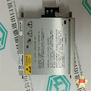
125840-01
The DSC1033 is a 3.3V fixed frequency MEMS
based PureSilicon™ Oscillator. It can be factory
programmed to any frequency from 1 to
150MHz.
The DSC1033 incorporates an all silicon
resonator that is extremely robust and nearly
immune to stress related fractures, common to
crystal based oscillators. Without sacrificing the
performance and stability required of today’s
systems, a crystal-less design allows for a
higher level of reliability, making the DSC1033
ideal for rugged, industrial, and portable
applications where stress, shock, and vibration
can damage quartz crystal based systems.
Available in industry standard packages, the
DSC1033 can be “dropped-in” to the same PCB
footprint as standard crystal oscillators.
Block Diagram
Standby#
PFD VCO
Frac-N
PLL
Resonator
V Output DD
GND
(pin1)
Standby#
PFD VCO
Frac-N
PLL
Resonator
V Output DD
GND
(pin1)
Features
Frequency Range: 1 to 150MHz
Exceptional Stability over Temperature
o ±25 PPM, ±50 PPM
Operating voltage
o 3.0 to 3.6V
Operating Temperature Range
o Industrial -40ºC to 85ºC
o Ext. Commercial -20ºC to 70ºC
o Commercial 0ºC to 70ºC
Low Operating and Standby Current
o 3mA Operating (40MHz)
o 1uA Standby
Ultra Miniature Footprint
o 2.5 x 2.0 x 0.85 mm
o 3.2 x 2.5 x 0.85 mm
o 5.0 x 3.2 x 0.85 mm
o 7.0 x 5.0 x 0.85 mm
Excellent Shock and Vibration
Resistance
Lead Free, RoHS & Reach SVHC
Compliant
Benefits
Pin for pin “drop in” replacement for
industry standard oscillators
Semiconductor level reliability,
significantly higher than quartz
Short mass production lead-times
Longer Battery Life / Reduced Power
Compact Plastic package
Cost Effective
Applications
Mobile Applications
Consumer Electronics
Portable Electronics
CCD Clock for VTR Cameras
Low Profile Applications
Industrial
All Rights Reserved. No part of this document may be copied or reproduced in any form without the prior written permission of Micrel, Inc. Micrel Inc. may update or make changes
to the contents, products, programs or services described at any time without notice. This document neither states nor implies any kind of warranty, including, but not limited to
implied warranties of merchantability or fitness for a particular use.
Page 2 MK-Q-B-P-D-031809-01-7
DSC1033 3.3V Low-Power CMOS Oscillator
Absolute Maximum Ratings1
Item Min. Max Unit Condition
Supply Voltage -0.3 +4.0 V
Input Voltage -0.3 VDD+0.3 V
Junction Temp - +150 °C
Storage Temp -55 +150 °C
Soldering Temp - +260 °C 40 sec max.
ESD
HBM
MM
CDM
-
2000
200
500
V
Ordering Code
Recommended Operating Conditions
Specifications
Notes:
1. Absolute maximum ratings are those values beyond which the safety of the device cannot be guaranteed. The device should not be
operated beyond these limits.
2. tSU is time to stable output frequency after VDD is applied. tSU and tEN (after EN is asserted) are identical values.
3. See typical cycle to cycle jitter graph for frequency dependence.
Parameter Symbol Range
Supply Voltage VDD 3.0 – 3.6V
Output Load ZL R>10KΩ, C≤15pF
Operating Temperature
Option 1
Option 2
Option 3
T -40 − +85 °C
-20 − +70 °C
0 − +70 °C
Parameter Symbol Condition Min. Typ. Max. Unit
Frequency f0 Single Frequency 1 150 MHz
Frequency Tolerance
Option 1
Option 2
Option 3 Δf
-40°C to +85°C
-20°C to +70°C
0°C to +70°C
±25,±50
±25,±50
±25,±50
ppm
Supply Current, no load IDD
CL=0p
RL=∞
T=25°
C
1 to 40MHz
40 to 80MHz
80 to 125MHz
125 to 150MHz
3
4
5
6 10 mA
Supply Current, standby IDD T=25°C 1.0 uA
Output Logic Levels
Output logic high
Output logic low
VOH
VOL
CL=15pF 0.8*VDD
-
-
0.2*VDD
Volts
Output Transition time
Rise Time
Fall Time
tR
tF
CL=15pF; T=25°C
20%/80%*VDD
1.3
1.3
2
2
ns
Output Startup Time2
tSU T=25°C 1.5 3 ms
Output Disable Time tDA 20 100 ns
Output Duty Cycle SYM 45 55 %
Input Logic Levels
Input logic high
Input logic low
VIH
VIL
0.75*VDD
-
-
0.25* VDD
Volts
Jitter, Cycle to Cycle JCC F = 100MHz3 95 ps
DSC1033 032.0000
Family
Output Freq
1.0 to 150MHz
CE1
Package, Temp
& Stability
- T
Tape/
Reel
* See Ordering Information for details
All Rights Reserved. No part of this document may be copied or reproduced in any form without the prior written permission of Micrel, Inc. Micrel Inc. may update or make changes
to the contents, products, programs or services described at any time without notice. This document neither states nor implies any kind of warranty, including, but not limited to
implied warranties of merchantability or fitness for a particular use.
Page 3 MK-Q-B-P-D-031809-01-7
DSC1033 3.3V Low-Power CMOS Oscillator
Nominal Performance Characteristics
3.3V Characteristics
Supply Current
0
4
8
12
16
0 50 100 150
Frequency (MHz)
Supply Current (mA)
Ta = 25°C 1pF 8pF 15pF
Standby Current
0
0.2
0.4
0.6
0.8
1
0 50 100 150
Frequency (MHz)
Standby Current (µA)
-40°C 25°C 85°C
Rise Time
0
0.5
1
1.5
2
0 50 100 150
Frequency (MHz)
Rise Time (ns)
-40°C 25°C 85°C
Fall Time
0
0.5
1
1.5
2
0 50 100 150
Frequency (MHz)
Fall Time (ns)
-40°C 25°C 85°C
Period Jitter
0
10
20
30
40
0 50 100 150
Frequency (MHz)
RMS Jitter (ps)
25°C
Cycle to Cycle Jitter
0
50
100
150
200
0 50 100 150
Frequency (MHz)
Jitter (ps)
25°C
All Rights Reserved. No part of this document may be copied or reproduced in any form without the prior written permission of Micrel, Inc. Micrel Inc. may update or make changes
to the contents, products, programs or services described at any time without notice. This document neither states nor implies any kind of warranty, including, but not limited to
implied warranties of merchantability or fitness for a particular use.
Page 4 MK-Q-B-P-D-031809-01-7
DSC1033 3.3V Low-Power CMOS Oscillator
Output Waveform
Standby Function
Standby#
(pin 1)
Output
(pin 3)
Hi Level Output ON
Open
(no connect) Output ON
Low Level High Impedance
Test Circuit
VOH
VOL
VIL
1/fo
Output
Standby#
tDA
tEN
tR tF
VIH
VDD 0.01uF 15pF
IDD
*VSD
4
1 2
3
*VSD = Standby# Logic Level Input
All Rights Reserved. No part of this document may be copied or reproduced in any form without the prior written permission of Micrel, Inc. Micrel Inc. may update or make changes
to the contents, products, programs or services described at any time without notice. This document neither states nor implies any kind of warranty, including, but not limited to
implied warranties of merchantability or fitness for a particular use.
Page 5 MK-Q-B-P-D-031809-01-7
DSC1033 3.3V Low-Power CMOS Oscillator
Board Layout (recommended)
Solder Reflow Profile
Package Dimensions
7.0 x 5.0 mm Plastic Package
MSL 1 @ 260°C refer to JSTD-020C
Ramp-Up Rate (200°C to Peak Temp) 3°C/Sec Max.
Preheat Time 150°C to 200°C 60-180 Sec
Time maintained above 217°C 60-150 Sec
Peak Temperature 255-260°C
Time within 5°C of actual Peak 20-40 Sec
Ramp-Down Rate 6°C/Sec Max.
Time 25°C to Peak Temperature 8 min Max.
Pin Terminal
VDD
Standby#
Output
GND
#1 #2
#4 #3
7.0±0.10 [0.276±0.004]
5.0±0.10 [0.197±0.004]
External Dimensions
#3 #4
5.08 [0.2]
#2 #1
1.2 [0.047]
1.4 [0.055]
0.85±0.05 [0.033±0.002]
Recommended Land Pattern*
1.4 [0.055]
1.4 [0.055]
5.08 [0.200]
units: mm [inch]
No.
4
1
3
2
0.2 [0.008]
2.6 [0.102] 2.6 [0.102]
0.2 [0.008]
2.2 [0.087]
3.5 [0.138]
o o
o o
o o
0.2 [0.008]
*Note: The center pad is not connected
internally and should be left unconnected or tied to GND.
60-150
Sec
20-40
Sec
60-180
Sec
8 min max
Pre heat
Reflow
Cool
Time
Temperature (°C)
3C/Sec Max.
6C/Sec Max.
200°C
217°C
150°C
25°C
260°C
3C/Sec Max.
60-150
Sec
20-40
Sec
60-180
Sec
8 min max
Pre heat
Reflow
Cool
Time
Temperature (°C)
3C/Sec Max.
6C/Sec Max.
200°C
217°C
150°C
25°C
260°C
60-150
Sec
20-40
Sec
60-180
Sec
8 min max
Pre heat
Reflow
Cool
Time
Temperature (°C)
3C/Sec Max.
6C/Sec Max.
200°C
217°C
150°C
25°C
260°C
3C/Sec Max.
All Rights Reserved. No part of this document may be copied or reproduced in any form without the prior written permission of Micrel, Inc. Micrel Inc. may update or make changes
to the contents, products, programs or services described at any time without notice. This document neither states nor implies any kind of warranty, including, but not limited to
implied warranties of merchantability or fitness for a particular use.
Page 6 MK-Q-B-P-D-031809-01-7
DSC1033 3.3V Low-Power CMOS Oscillator
5.0 x 3.2 mm Plastic Package
3.2 x 2.5 mm Plastic Package
Pin Terminal
VDD
Standby#
Output
GND
0.85±0.05 [0.033±0.002]
Recommended Land Pattern
#1 #2
#4 #3
3.2±0.05 [0.126±0.002]
2.5±0.05 [0.098±0.002]
#3 #4
#2 #1
0.8±0.1 [0.031±0.004]
0.9±0.05 [0.035±0.002]
CO.25
1.0 [0.039]
0.9 [0.035]
2.1 [0.083]
No
.
4
1
3
2
2.1 [0.083]
External Dimensions
units: mm [inch]
0.9 [.035] 0.9 [0.035]
0.2 [0.008]
Pin Terminal
VDD
Standby#
Output
GND
#1 #2
#4 #3
5±0.10 [0.197±0.004]
3.2±0.10 [0.126±0.004]
External Dimensions
#3 #4
2.54 [0.100]
#2 #1
0.9 [0.035]
1.2 [0.047]
0.85±0.05 [0.033±0.002]
Recommended Land Pattern
1.1 [0.043]
1.2 [0.047]
2.54 [0.100]
units: mm [inch]
No.
4
1
3
2
0.2 [0.008]
0.1 [0.004]
2.1 [0.083] 1.2 [0.047]
0.1 [0.004]
All Rights Reserved. No part of this document may be copied or reproduced in any form without the prior written permission of Micrel, Inc. Micrel Inc. may update or make changes
to the contents, products, programs or services described at any time without notice. This document neither states nor implies any kind of warranty, including, but not limited to
implied warranties of merchantability or fitness for a particular use.
Page 7 MK-Q-B-P-D-031809-01-7
DSC1033 3.3V Low-Power CMOS Oscillator
2.5 x 2.0 mm Plastic Package
Ordering Information
DSC1033 PTS – xxx.xxxx T
PART NUMBERING GUIDE
Package
(Plastic QFN) Temperature Stability Frequency Packing Option
P=A: 7.0x5.0mm
P=B: 5.0x3.2mm
P=C: 3.2x2.5mm
P=D: 2.5x2.0mm
T=C: 0
o ~ +70o C
T=E: -20o ~ +70o C
T=I: -40o ~ +85o C
S=1: ±50ppm
S=2: ±25ppm
XXX.XXXX
(4 decimal places)
Blank: Tubes
- T: Tape & Reel
Example: DSC1033CE1–123.0000T
The example part number above is a 123.0000MHz oscillator in Plastic 3.2x2.5mm package, with ±50ppm
stability over an operating temperature of -20 to +70oC, shipped in Tape and Reel. The reel size (7” or 13”
diameter) will be determined by the factory based on quantity.
Disclaimer:
Micrel makes no representations or warranties with respect to the accuracy or completeness of the information furnished in this data sheet. This information is not intended as a
warranty and Micrel does not assume responsibility for its use. Micrel reserves the right to change circuitry, specifications and descriptions at any time without notice. No
license, whether express, implied, arising by estoppel or otherwise, to any intellectual property rights is granted by this document. Except as provided in Micrel’s terms and
conditions of sale for such products, Micrel assumes no liability whatsoever, and Micrel disclaims any express or impl
Tolerance
class
Nominal sizes
2 to 30
>30
up to
120
>120
up to
400
>400
up to
1000
>1000
up to
2000
>2000
up to
4000
>4000
up to
8000
>8000
up to
12000
>12000
up to
16000
>16000
up to
20000
>20000
Tolerances
A
± 1
± 1 ± 1 ± 2 ± 3 ± 4 ± 5 ± 6 ± 7 ± 8 ± 9
B ± 2 ± 2 ± 3 ± 4 ± 6 ± 8 ± 10 ± 12 ± 14 ± 16
C ± 3 ± 4 ± 6 ± 8 ± 11 ± 14 ± 18 ± 21 ± 24 ± 27
D ± 4 ± 7 ± 9 ± 12 ± 16 ± 21 ± 27 ± 32 ± 36 ± 40
INSTRUCTION SHEET Identification: INS-033.1
TMA Standard Tolerances Page: 13/17
6.2 Tolerances on Angular Dimensions
As per EN ISO 13920 Class B:
Tolerance class
Nominal sizes
up to 400 > 400 up to 1000 > 1000
Tolerances
A ± 20’ ± 15’ ± 10’
B ± 45’ ± 30’ ± 20’
C ± 1° ± 45’ ± 30’
D ± 1° 30’ ± 1° 15’ ± 1°
Calculated and rounded tolerances (in mm/m) 1
A ± 6 ± 4.5 ± 3
B ± 13 ± 9 ± 6
C ± 18 ± 13 ± 9
D ± 26 ± 22 ± 18
1) The value indicated in mm/m must be multiplied by the length in meters of the shorter leg.
6.3 Straightness, Flatness, and Parallelism Tolerances
As per EN ISO 13920 Class F:
Tolerance
class
Nominal sizes
> 30 up
to 120
> 120
up to
400
> 400
up to
1000
> 1000
up to
2000
> 2000
up to
4000
> 4000
up to
8000
> 8000
up to
12000
> 12000
up to
16000
> 16000
up to
20000
> 20000
Tolerances
E 0.5 1 1.5 2 3 4 5 6 7 8
F 1 1.5 3 4.5 6 8 10 12 14 16
G 1.5 3 5.5 9 11 16 20 22 25 25
H 2.5 5 9 14 18 26 32 36 40 40
7 Shot-blasting
The quality of shot-blasting is as follows:
- Cleanliness or degree of preparation Sa 2 ½ (ISO 8501-1)
- Medium roughness (NF EN ISO 8503)
8 Indications for Measurement
8.1 Oxyfuel and Laser Cut Pieces
Measurements should be taken on oxide-free cut surfaces away from imperfections. Cut edges should be clean
and even.
INSTRUCTION SHEET Identification: INS-033.1
TMA Standard Tolerances Page: 14/17
8.2 Stampings
Stampings are, by definition, subjected to deformation during the manufacturing process (see diagram below).
Measurements should be taken from non-deformed zones.
Diagram of a stamping
8.3 Angle Measurements
8.3.1 Height of a Bent Edge
The zone measured should be no farther than 5 mm from the zone affected by the bending deformation (see
diagram below).
In other words, measurements should be taken as close as possible to the bend, but not in it (which would
invalidate the result).
Measurement zone for the height of a bent edge
Actual size : length or diameter
Break band
Cut band
Draw-in band
Break band
Height
of
sheared
face
Depth of burr.
Actual size : length or diameter
Measurement zone
Height
INSTRUCTION SHEET Identification: INS-033.1
TMA Standard Tolerances Page: 15/17
8.3.2 Distance between Two Bent Edges
Apply the same rules as for the measurement of the height of a bent edge. Measurements should be taken at
the base of the bend and away from the deformed zone (see diagram below).
Measurement zone for the outer distance between two bent edges
Measurement zone
INSTRUCTION SHEET Identification: INS-033.1
TMA Standard Tolerances Page: 16/17
8.4 Flatness
The work piece should be positioned against the straightedge for minimal deflection (best-case scenario).
Deflection should be measured between the concave (inner) surface of the work piece and the straightedge (or
marble).
Measurement of flatness defects: maximum deflection “f”
If the straightedge is longer than the work piece, flatness should be measured for the entire work piece.
If the straightedge is shorter than the work piece, measurements should be relative to the length of the work
piece covered by the straightedge.
Straightedge longer than work piece Work piece longer than straightedge
Work piece
Marble
Straightedge
Straighedge
Not measured
Piece
Straighedge
Piece
INSTRUCTION SHEET Identification: INS-033.1
TMA Standard Tolerances Page: 17/17
8.5 Coaxiality
One approximate method involves measuring the differences between opposing radii on two orthogonal
planes. The difference between xi and yi should be no greater than the coaxiality tolerance (0.8 in the example
below).
Example specifications Approximate approach for verifying
coaxiality tolerance
In the example above, measurements are as follows:
x1 = 31, y1 = 31.6, x2 = 31.3, y2 = 31.4
Therefore: |x1 - y1| = 0.6 ≤ 0.8 and |x2 - y2| = 0.1 ≤ 0.8 → Coaxiality is compliant.
8.6 Symmetry
One approximate method involves measuring differences in width orthogonally to the axial plane. The
difference between xi and yi should be no greater than the tolerance “t”.
Approximate method for verifying symmetrical tolerance
Distribution
All TMA suppliers for aluminum sheet metal
President Tech. Officer TMA x Dir. of Purchasing/Sub-con x Methods / Design Office x
Dir. of Finance x Tech. Officer LDA x Info/Sched. Manager x
Dir. of Sales x Tech. Officer RDA x Tech. Officer CHELLES X
Dir. of Operations x Tech. Officer TAS x Tech. Officer NEOTEC x
Index Date Modified Written Verified Approved
1 29/07/19 Intégration GED - - -
B 08/01/08 OXY standard reference S


闽公网安备 35020302034948号


 收藏商品
收藏商品

 QQ咨询
QQ咨询
 当前商品暂无此评价~
 2778087246
 18150367963


 记住账号
记住账号