¥ 1495.00
¥ 1495.00
¥ 1495.00
¥ 1495.00
¥ 1495.00
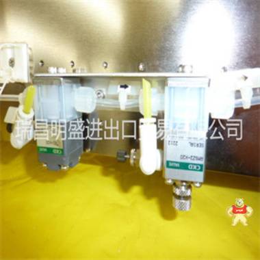
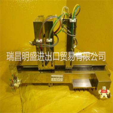
易卖工控网(www.ymgk.com)提供”716-011638-498740模块备件”,产品详情:品牌/厂家:、型号:716-011638-498740、成色:全新、货期:现货 1天内发货、保修:180天,更多产品详情就上易卖工控网。
716-011638-498740
6.1大额定值
超过虚拟结温度范围(除非另有说明)(1)
小大单位
VIN连续输入电压范围(3)–0.3 16 V
冯/关开/关输入电压范围–0.3 16 V
输出电压范围(2)–0.3 9 V
IO输出电流(4)内部受限
(短路保护)-
RθJA封装热阻抗(4)(5)206°C/W
TJ工作虚拟结温度150°C
Tstg储存温度范围–65 150°C
(1) 超过大额定值的应力可能会对设备造成久性损坏。这些是压力等级
仅在这些或任何其他条件下,设备的功能运行超出推荐运行条件
不暗示条件。长时间暴露在大额定条件下可能会影响设备的可靠性。
(2) 如果负载返回到双电源系统中的负电源,则输出必须是二极管箝位到GND。
(3) PNP通过晶体管在输入和输出之间连接有一个寄生二极管。该二极管通常为反向偏置
(VIN>VOUT),但如果输出电压超过输入电压一个二极管压降,则为正向偏置(参见应用和
更多详细信息,请参见实施部分)。
(4) 大功耗是TJ的函数
(max)、RθJA和TA。在任何允许的
环境温度为PD=(TJ
(max)–TA)/RθJA。在大TJ下运行
150°C会影响可靠性。
(5) 根据JESD 51-7计算封装热阻抗。
6.2 ESD额定值
价值单位
V(ESD)静电放电
人体模型(HBM),符合ANSI/ESDA/JEDEC JS-001,所有引脚(1)2000
充电设备型号(CDM),符合JEDEC规范JESD22-C101,V
所有销(2)1000
(1) JEDEC文件JEP155规定,500-V HBM允许通过标准ESD控制过程进行安全制造。
(2) JEDEC文件JEP157指出,250-V CDM允许通过标准ESD控制过程进行安全制造。
6.3推荐操作条件
小大单位
VIN电源输入电压2.2(1)16 V
VON/OFF ON/OFF输入电压0 VIN V
输出电流150 mA
TJ虚拟结温度–40 125°C
(1) 对于工作IL,建议的小VIN为2.5 V或VOUT(大)+额定压降(大)中的较大值。
6.4热信息
热计量(1)
LP2985
DBV装置
5针
RθJA结对环境热阻205.4°C/W
RθJC(顶部)结至外壳(顶部)热阻78.8°C/W
RθJB接线板热阻46.7°C/W
ψJT结至顶部表征参数8.3°C/W
ψJB接线板特性参数46.3°C/W
(1) 有关传统和新热指标的更多信息,请参阅半导体和IC封装热指标应用程序
汇报
LP2985
SLVS522P–2004年7月–2022年2月修订www.ti。通用域名格式
4提交文件反馈版权所有©2022 Texas Instruments Incorporated
716-011638-498740

716-011638-498740
6.1 Absolute Maximum Ratings
over virtual junction temperature range (unless otherwise noted)(1)
MIN MAX UNIT
VIN Continuous input voltage range(3) –0.3 16 V
VON/OFF ON/OFF input voltage range –0.3 16 V
Output voltage range(2) –0.3 9 V
IO Output current(4) Internally limited
(short-circuit protected) —
RθJA Package thermal impedance(4) (5) 206 °C/W
TJ Operating virtual junction temperature 150 °C
Tstg Storage temperature range –65 150 °C
(1) Stresses beyond those listed under absolute maximum ratings may cause permanent damage to the device. These are stress ratings
only, and functional operation of the device at these or any other conditions beyond those indicated under Recommended Operating
Conditions is not implied. Exposure to absolute-maximum-rated conditions for extended periods may affect device reliability.
(2) If load is returned to a negative power supply in a dual-supply system, the output must be diode clamped to GND.
(3) The PNP pass transistor has a parasitic diode connected between the input and output. This diode normally is reverse biased
(VIN > VOUT), but is forward biased if the output voltage exceeds the input voltage by a diode drop (see the Application and
Implementation section for more details).
(4) Maximum power dissipation is a function of TJ
(max), RθJA, and TA. The maximum allowable power dissipation at any allowable
ambient temperature is PD = (TJ
(max) – TA) / RθJA. Operating at the absolute maximum TJ
of 150°C can affect reliability.
(5) The package thermal impedance is calculated in accordance with JESD 51-7.
6.2 ESD Ratings
VALUE UNIT
V(ESD) Electrostatic discharge
Human body model (HBM), per ANSI/ESDA/JEDEC JS-001, all pins(1) 2000
Charged device model (CDM), per JEDEC specification JESD22-C101, V
all pins(2) 1000
(1) JEDEC document JEP155 states that 500-V HBM allows safe manufacturing with a standard ESD control process.
(2) JEDEC document JEP157 states that 250-V CDM allows safe manufacturing with a standard ESD control process.
6.3 Recommended Operating Conditions
MIN MAX UNIT
VIN Supply input voltage 2.2(1) 16 V
VON/OFF ON/OFF input voltage 0 VIN V
IOUT Output current 150 mA
TJ Virtual junction temperature –40 125 °C
(1) Recommended minimum VIN is the greater of 2.5 V or VOUT(max) + rated dropout voltage (max) for operating IL.
6.4 Thermal Information
THERMAL METRIC(1)
LP2985
DBV UNIT
5 PINS
RθJA Junction-to-ambient thermal resistance 205.4 °C/W
RθJC(top) Junction-to-case (top) thermal resistance 78.8 °C/W
RθJB Junction-to-board thermal resistance 46.7 °C/W
ΨJT Junction-to-top characterization parameter 8.3 °C/W
ΨJB Junction-to-board characterization parameter 46.3 °C/W
(1) For more information about traditional and new thermal metrics, see the Semiconductor and IC Package Thermal Metrics application
report.
LP2985
SLVS522P – JULY 2004 – REVISED FEBRUARY 2022 www.ti.com
4 Submit Document Feedback Copyright © 2022 Texas Instruments Incorporated


闽公网安备 35020302034948号


 收藏商品
收藏商品

 QQ咨询
QQ咨询
 当前商品暂无此评价~


 2778087246
 18150367963


 记住账号
记住账号